W25Q40CLSNIG SPI Flash
Overview
The Boardoza W25Q40CLSNIG is a high-performance non-volatile memory expansion module designed to provide reliable code and data storage for embedded systems. At its core lies the Winbond W25Q40CL Serial Flash memory engine, a 4-Megabit (512 Kilobyte) device engineered for space-constrained applications requiring fast random access and low power consumption.
This breakout board serves as a robust "digital locker" for microcontrollers, enabling them to store firmware images (for Over-The-Air updates), configuration parameters, or high-speed sensor logs. By utilizing the standardized SPI (Serial Peripheral Interface) bus, it offers a seamless storage upgrade for platforms lacking sufficient internal flash, such as legacy 8-bit MCUs or modern IoT nodes.

Core Technical Specifications
The module is defined by the following operational parameters:
Memory Density: Provides 4 Megabits (512 KB) of storage organized into uniform 4KB erasable sectors and larger 32KB/64KB blocks.
Data Throughput: Supports high-speed SPI clock frequencies up to 104 MHz, enabling rapid data retrieval for execution-in-place (XIP) architectures.
Operating Voltage: Features a flexible input range of 3.3V to 5V DC, facilitating direct integration with both low-voltage logic and standard 5V legacy systems.
Durability and Retention: Rated for over 100,000 program/erase cycles with data retention exceeding 20 years, ensuring long-term reliability in industrial deployments.
Power Efficiency: Optimized for battery-operated devices, with active current consumption as low as 1 mA and deep power-down currents in the micro-ampere range.
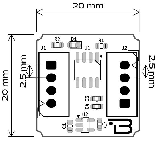
Physical Dimensions: A compact 20 mm x 20 mm square footprint designed for tight enclosure integration.
Key Engineering Features
Enhanced SPI Modes (Dual/Quad I/O)
While the module defaults to standard SPI (Clock, Chip Select, Data In, Data Out), the W25Q40CL engine supports Dual and Quad SPI modes. By utilizing the Write Protect (/WP) and Hold (/HOLD) pins as additional bidirectional data lines (IO2 and IO3), the effective data transfer rate can be quadrupled, significantly reducing boot times for complex firmware.
Flexible Sector Architecture
The memory array is divided into 4KB uniform sectors, which allows for granular data management. This architecture is particularly beneficial for applications requiring frequent updates to small data packets—such as storing user settings or calibration constants—without needing to erase large blocks of memory, thereby extending the overall lifespan of the chip.
Integrated Visual Diagnostics
Unlike bare chips, this breakout board includes an onboard Power LED (D1). This provides immediate visual confirmation of power rail integrity during prototyping and field diagnostics, eliminating guesswork during initial system bring-up.
Hardware Interface and Signal Mapping
The module interfaces via two distinct headers (J1 and J2) to separate basic communication from advanced control features:
Primary Interface (J1)
5V: Positive power supply input. The board regulates this for the internal memory logic.
CLK: Serial Clock Input. Driven by the host microcontroller to synchronize data transmission.
DI: Data Input (MOSI). The line carrying data/commands from the host to the memory.
GND: Common system ground.
Advanced Control (J2)
CS: Chip Select (Active Low). Must be driven low to initiate any communication with the device.
DO: Data Output (MISO). The line carrying data from the memory back to the host.
WP: Write Protect. An active-low pin used to hardware-lock specific memory regions against accidental overwrites.
HOLD: Hold Input. Allows the host to pause communication without deselecting the device, useful in multi-slave SPI bus topologies.
Applications
Firmware-Over-The-Air (FOTA): Staging area for downloading new system updates before flashing the main MCU.
Data Logging: Non-volatile buffer for sensors recording environmental metrics like temperature or vibration.
Asset Configuration: Storing lookup tables, bitmap graphics, or font libraries for display modules.
FPGA Configuration: Storing the bitstream required to configure Field Programmable Gate Arrays at power-up.
Board Dimensions:

Ready to integrate? You can purchase the W25Q40CLSNIG SPI Flash directly from ourOnline Store . Worldwide shipping is available for engineering samples and production batches.
Last updated
